Whereas commands in high level languages such as Java or Python embody logical concepts (e.g. “if [this event] occurs, execute [this code]”), assembly language machine instructions correlate directly to the functions of a processor chip. So, assembly machine instructions can be directly translated into the sequences of 1s and 0s read by the computer processor, called machine language. The data involved in assembly programs are also sequences of 1s and 0s, generally notated in hexadecimal for the sake of readability.
Project Notes
The following describes major ideas I considered while writing the assembly code for the multiplication and screen fill programs specified in Project 04.
Nand2Tetris Assembly Language Conventions
Nand2Tetris assembly is particular because each machine instruction, being only 16 bits long, cannot encode operands as part of the instruction. Therefore, operands must be loaded into designated registers, called the D (data) and A (address) registers, before operations can commence. Also, programs need to be “terminated” with infinite loops—probably so that the test script ends, and thus so does the program.
Marked Mistakes
On several occasions, I’d do a calculation, store the result in the D register, but then forget to store it in a different register, meaning the result of the calculation would be overriden by the next. I’d also sometimes get confused as to whether I was working with the address of a register or the data in it, but managed to figure things out by running it on the emulator.
I also struggled a lot more on the screen fill program than the multiplication one. I think my mistake was that I ran a loop to check for key presses, but then tried to jump from that loop to a different loop which would either fill or erase the screen. What ended up working was writing a loop that’d run through the “check for key presses” code on every cycle, which meant that the program could detect a key being pressed and held, and change pixels on the screen for as long as it continues to detect a key being held.
I commented both programs for this project pretty extensively. You can view them here.
Further investigation I can do on the topic of assembly language are likely better done with other textbooks and languages, so I think I can move onto the next project now.
A combinational circuit is one whose output does not depend on the value of the previous output, whereas a sequential circuit is one whose output does. Because computer memory requires data to be retained over time, it is inherently time-dependent, and must be built with sequential logic gates.
The sequential circuitry used in the Nand2Tetris ‘Hack’ computer is called the data flip-flop, which “remembers” the bit (either 0 or 1) inputted in the previous time unit.
Project Notes
The following describes major ideas I considered while writing the HDL for the register, memory, and program counter chips specified in Project 03.
NOTE 12/13/23, revisiting Nand2Tetris: This section has been cut short since I finished this project in May 2023, but did not leave much commentary, nor do I remember much about the process of working on it. Mostly, I recall initially struggling to understand the function of a DFF gate in a way where I could manipulate it to construct the specified sequential chips. I also found the hint in the Nand2Tetris textbook about building larger RAM chips using recursion very helpful, so if you’re working on this project as well, I’d highly suggest you check that out. Don’t skip the textbook! Anyways, that’s it. I’m off to finish what I’d started on the next project.
Here’s a follow-up of the “Simplifying Circuits” inquiry from my Nand2Tetris Project 01 post.
So, I was a little confused by the posts I’d read, which implied that a truth table can directly make clear the simplest way to notate a Boolean function. After searching around online, I found that a Karnaugh map, or k-map, is probably the “truth table” people were referring to. The k-map technique involves drawing out 2D representations of Boolean functions so that logical adjacencies become visually evident. Here is how I simplified DMux using the technique.
(I’d read in a forum that Xor is most minimally built in 4 Nand gates, which is why I knew to notate that Xor == 4 Nands before having actually simplified it myself.)
As for the other two chips that needed simplification, Xor and Mux, I found that an algebraic approach was more suitable than a graphical one. After reading the Boolean algebra chapter of The Art of Assembly Language, and playing around with the canonical forms of Xor and Mux, I figured out how to reduce the chips to a minimal number of Nand gates.
Now, I have all the fundamental chips from Project 01 (And, Dmux, Mux, Not, Or, and Xor) built using the simplest possible configurations of Nand gates. If you like, you can view my code on Github.
Most computer systems represent signed integers using a method called 2’s complement, where, in a fixed number of bits, negative integers are represented using the negation of their absolute value plus 1. This method is convenient for a number of reasons:
Negative integers can seamlessly be included in binary addition operations.
There is only one possible representation of 0.
The most significant bit of any integer indicates its sign (0 for positive integers, and 1 for negative integers).
The arithmetic logic unit (ALU) is a computer chip that performs arithmetic and bitwise operations on integers represented in 2’s complement.
Project Notes
The following describes major ideas I considered while writing the HDL for the adder, incrementer, and ALU chips specified in Project 02.
Definition of NAND
Briefly had this misconstrued while building FullAdder.
NAND is NOT(A AND B), not (NOT A) AND (NOT B).
ALU in <20 lines of HDL?
(It’s stated in the course materials that the ALU can be specified in less than 20 lines of HDL, so I wanted to achieve that.)
I’d originally tried to “zero” inputs by AND’ing them with NOT zx (or for the y-input, NOT zy), but of course, ran into the “different bus widths” error. Then, it hit me that I could write a Mux16 with a=input, b=false, and sel=zx (or NOT zy, for the y-input). In general, I’d forgotten about some of the chips I’d previously built, and was stuck until it hit me that they existed.
I also found myself running into the “sub bus of an internal node” error several times while writing the HDL for detecting zero or negative outputs. It worked after some syntactical adjustments, though. I used two 8-way ORs, an OR, and a NOT to detect zeros, and simply outputted the “out” value’s most significant bit to detect negatives.
Ultimately, I ended up with a pretty clean 15 lines of HDL.
Topics for further investigation:
Carry-lookahead Adder
I want to try building an adder that can detect whether a bit pair will generate or propagate a carry.
All boolean functions can be represented by “listing” every combination of inputs that result in an output of 1, like so:
OR(a, b) = a⋅b + ā⋅b + a⋅b̅
This is the canonical notation of the OR function. It indicates that OR(a, b) will return true when a AND b is true, OR when (NOT a) AND b is true, OR when a and (NOT b) is true.
Because all boolean functions can be represented with the binary operations AND, NOT, and OR, any logic gate can be constructed using the gates NAND and NOR. These gates are referred to as primitive because they can be used as the building blocks for more complex functions, and because they are the most physically simple.
Project Notes
The following describes major ideas I considered while writing the HDL for the 15 chips listed in Project 01.
From AND to AND16
Is using 16 AND gates to build the AND16 operation the most efficient approach?
Hardware description language (HDL) is a specification of the parts of a computer chip, not a calling of operations like in high-level programming.
Though it appears redundant, it’d make sense that the HDL for the AND16 operation specify 16 different AND gates, because that way, 16 bits can be operated upon in parallel.
Additional note: A system bus is just a different way to think of a set of n bits being operated upon, so it really does just require the use of n gates.
4-way and 8-way MUX16
In hindsight, I feel incredibly stupid for this. But, I spent a while wrestling with a bunch of irrelevant gates until I realized I could write 4-way and 8-way MUX16 with only several MUX16 gates. I also forgot that the buses are indexed right to left instead of vice versa, which also got me stuck for a while. Thankfully, this means I probably won’t be making similar mistakes again.
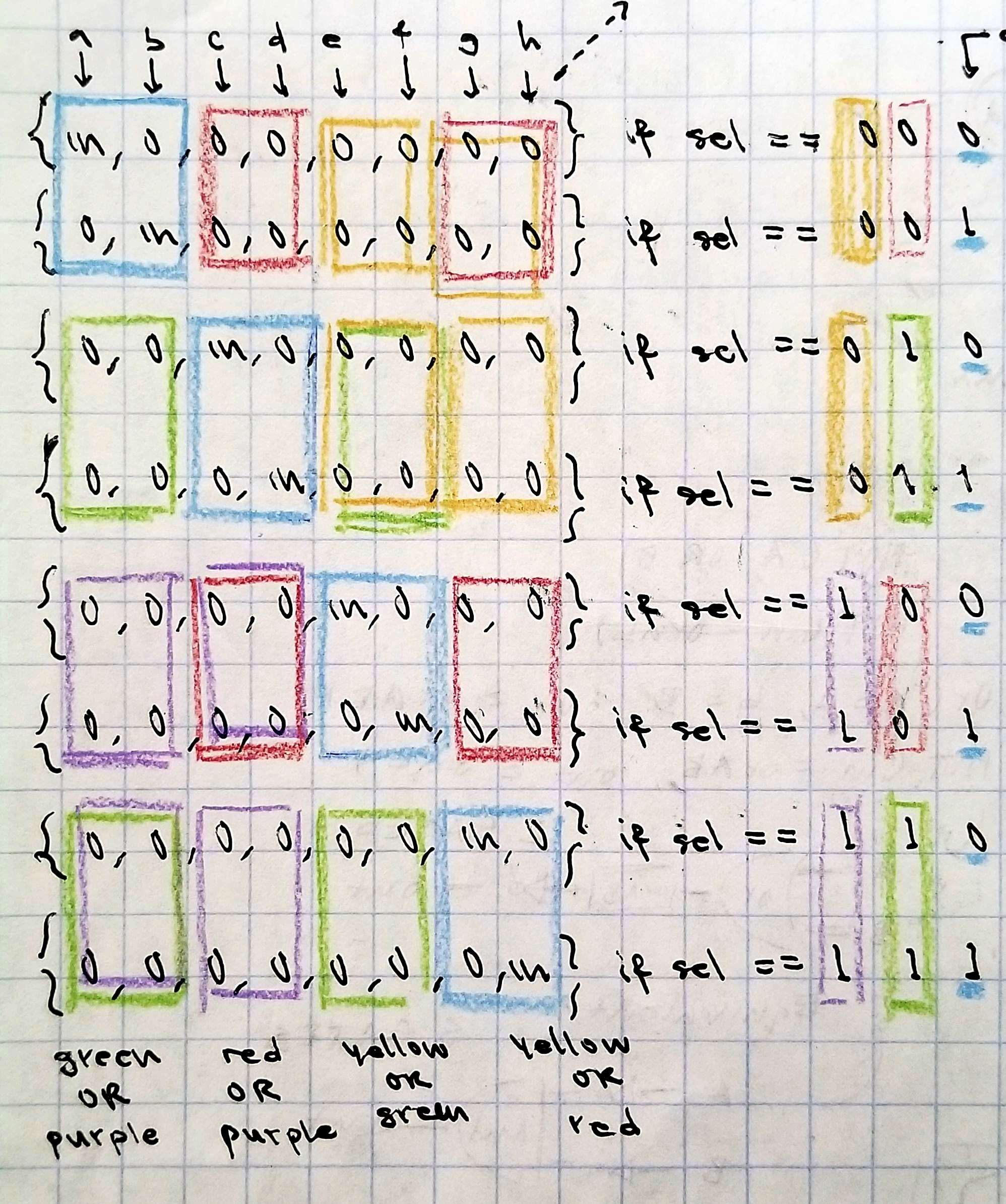
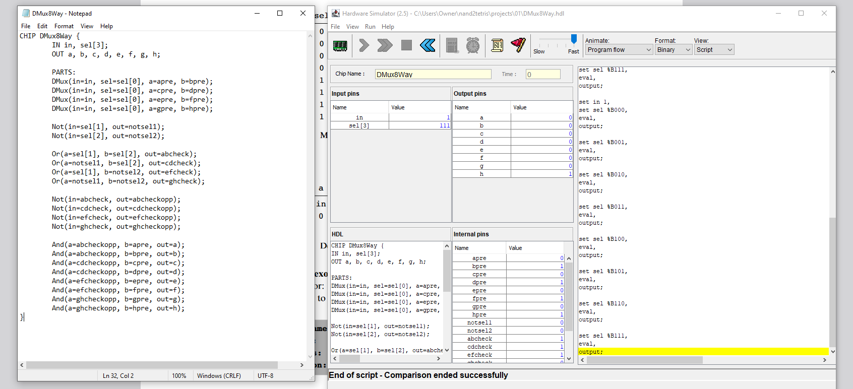
8-way DMUX
Think it’s worth mentioning that I had the most fun figuring this one out :)
(Click an image to view it in full.)
Topics for further investigation:
Simplifying Circuits
I read on EE StackExchange that someone used truth tables and DeMorgan’s laws to simplify all the chips as much as possible, and want to figure out the specifics of how to do that.
I’d like to rewrite the basic boolean operations I constructed from NAND gates in NOR gates to see which is more efficient. I figure if the OR operation could be done in 2 NOR gates instead of 3 NAND gates, there might also be better ways to write the other operations. However, the Nand2Tetris software suite doesn’t come with a built-in NOR the way it has built in NANDs, so I’ll see if I can come back to this once I’m familiar enough with the Nand2Tetris software to set it up myself.
UPDATE: I think I understand the concepts well enough to be able to drop this inquiry.

 Blog
Blog